
The center for information photonics and energy materials, founded in 2008, focuses on the growth of high performance optoelectronic thin film materials and the fabrication of photovoltaic energy conversion devices, energy storage devices, sensors and imaging device. Research topics of the group includes but not limited to (1) CIGS, CZTS thin film photovoltaic devices,(2) visible and near infrared broad band photo-detector, (3) X ray flat panel detector, (4) solid state lithium ion battery,(5) IGZO thin film transistor,(6) scanning probe microscopic characterization, (7)perovskite nanostructures, (8) barrier film for oxygen and moisture, (9) intelligent force and chemical sensors.
As of 2016, the group has been successfully awarded with 75 national and regional research projects with a total funding amount of more than 70 million RMB, including a 973 projects (28M RMB) from the Ministry of science and technology and a major equipment project of the Chinese Academy of Sciences. Using "three-stage" evaporation, the group has successfully fabricated CIGS with efficiency of 21.3% which is the first lab result who achieved 20%+ efficiency for thin film solar cell in China. The device performance is very close to that of the champion devices of efficiency above 22% made by ZSW and solar frontier. A CIGS pilot line of 40cmX60cm panel size has been designed and built using patented process and self-developed equipment, actively pushing the research achievements to commercialization. For the earth abundant CZTS solar cells, the team has revealed the detrimental effect from potential fluctuation of the band structure and developed a novel process to suppress the potential fluctuation which leads a CZTS solar cell efficiency improvement to 12.3%.
High efficiency CuIn1-xGaxSe2 (CIGS) thin film solar cells
CuIn1-xGaxSe2 (CIGS) thin film solar cells have been recognized as the most efficient thin-film solar cell, which is fabricated both on rigid substrate such as glass and on flexible substrate such as polyimide (PI). With these advantages such as low cost in fabrication of absorbing layer (thickness ~ 1.0-2.5 microns), light weight, high power density (up to 1100 W/kg in flexible cell), flexible CIGS, high performance for weak-light, long life and strong radiation resistance, CIGS solar cells exhibits the extensive application prospects as shown in Figure 1.
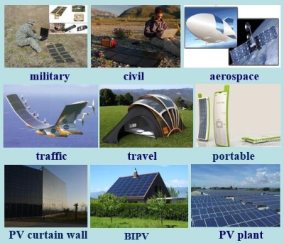
Figure 1. CIGS solar cells exhibits the extensive application prospects.
The center is dedicated to the independent research and development of commercial CIGS thin film solar cell devices, processes and core equipment, including glass substrate and flexible substrate devices.(1)Glass substrate CIGS solar cells. The device structure is shown in Figure 2. At present, through the improvement of the "three-stage " CIGS growth process, we have realized the band design helpful for the current collection, fabricated the absorption layer material of CIGS with high quality, and improved the device open circuit voltage by the defect passivation on the surface of CIGS by alkali metal postdeposition annealing. As a result, the conversion efficiency of CIGS cell devices reaches to 21.3%, the performance parameters are shown in Figure 3. Furthermore, the high efficiency device technology was transplanted to the production line. The pilot line of a large area of CIGS product has been designed and operated.
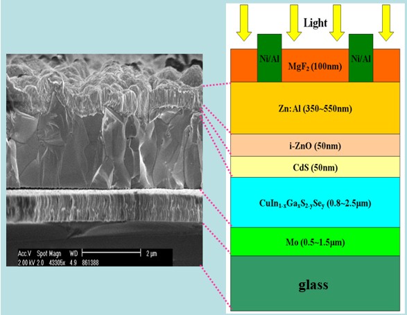
Figure 2. The structure diagram of CIGS solar cell.
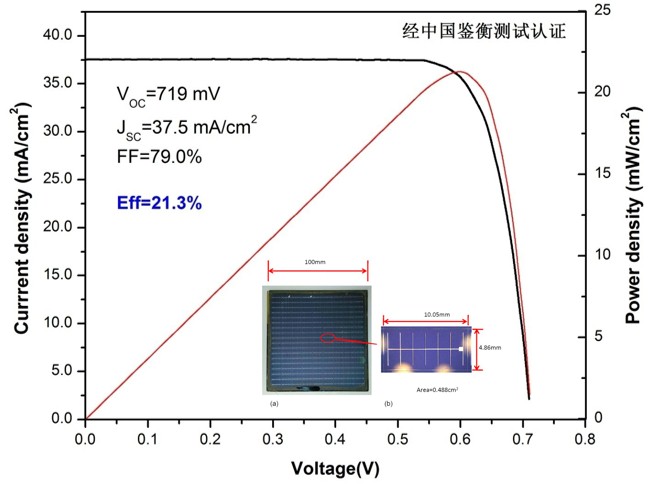
Figure 3. The performance parameters of CIGS with the conversion efficiency of 21.3%.
(2)Flexible CIGS solar cells. The center has developed a flexible transfer technology based on the rigid substrate, as shown in Figure 3. First, the high-temperature paint is coated on a glass substrate, forming a peeling layer. After that, the high-temperature PI film is synthesized on this peeling layer. And then, the functional layers of CIGS are fabricated on the PI film based on the "three-stage " CIGS growth process. Finally, the flexible CIGS solar cell is obtained by peeling the packaged flexible CIGS module from the glass substrate. This technology makes the flexible CIGS solar cells thinner, lighter and softer. At present, the conversion efficiency of flexible CIGS solar cell fabricated based on our technology is up to 16.3%, as shown in Figure 5.
Figure 4. The flexible transfer technology based on the rigid substrate

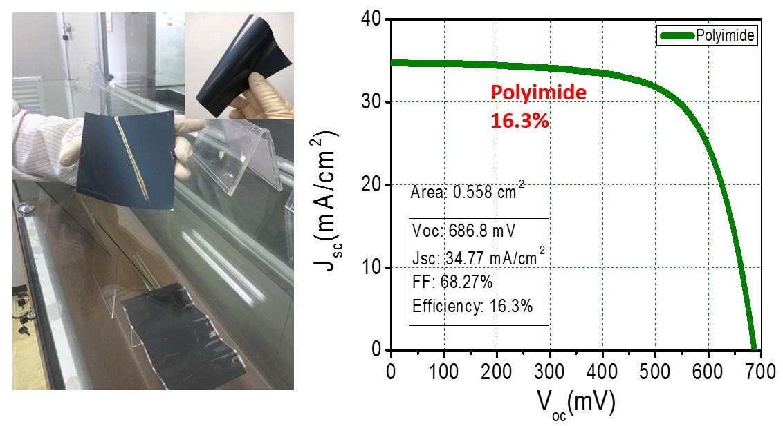
Figure 5. The fabricated flexible CIGS solar cell on PI substrate and the performance parameters.
Kesterite Cu2ZnSnS4 (CZTS) thin film solar cells
Kesterite Cu2ZnSnS4 (CZTS) thin film solar cells have attracted considerable interests in the last decade and have shown potential to replace its well-developed predecessor Cu(In,Ga)Se2 solar cell with earth-abundant and environmentally friendly raw materials. The CZTS thin films in our study are fabricated by a two-stage process consisting of precursor deposition by co-sputtering and post-sulfuration treatment which is a suitable method for high volume manufacturing.
We have systematically studied the dependence of Cu/Sn ratio in the prepared films on post-sulfuration parameters such as the peak annealing temperature, H2S concentration in the annealing atmosphere, temperature ramping rate. And a novel low temperature Cu2ZnSnS4 (CZTS) formation path is further designed which led to cell with power conversion efficiency of 8.58% (Figure 1). This process wisely separates the phase formation and crystal coalescence, which makes the fabrication of CZTS film be more controllable. Furthermore, the demonstration of the low temperature formation path provides new opportunities to fabricate high efficiency, cost-effective and environmental friendly CZTS solar cells on low weight and flexible substrates such as polyimide.
To investigate the influence of deep-level defects on the voltage deficit, the isoelectronic element Cd is doped to study the change of the potential fluctuation. It is found that the doping of Cd could suppress the formation of deep-level defect ZnCu due to the dimension effect. The potential fluctuation is reduced from 210mV to 98mV resulting in a greatly improved efficiency of 12.3% (Figure 2).
New visible-NIR broadband detector
Photodetectors with outstanding detecting over a broad spectral range have merit Based on the photoelectric effect, different technologically important wavelength regimes are detected by the separate photoactive semiconductors with suitable bandgaps. For example, commercially available photodetectors are typically made from GaP, Silicon and InGaAs for sensing in the ultraviolet (UV), visible and NIR regimes, respectively. Using different wavebands of detectors, the measured data and images should be processed with combination and optimization. The complex data processing and probable image distortion would hinder the application in precise instruments and imaging techniques. Furthermore, the multi-detector system is not convenient for optical path design and integration. So the photodetectors with broadband spectral response and high detectivity at room temperature are urgently needed, especially in some typical applications such as the portable spectral detector and ultraviolet to near-infrared digital camera.
In our study, the Cu2Zn1-xCdxSnSe4 photodetector has designed and achieved the detection broadband range over UV region from NIR region by tuning the bandgap of the Cu2Zn1-xCdxSnSe4 film according to doping the Cd content. The responsivity and detectivity of present photodetector were investigated in the range from 305 nm to 1554 nm (Figure 1) and the maximum values of 0.849 W/A and 6.86 × 10¹¹ Jones (Figure 2), respectively. Based on low cost, large area and broadband responsivity, this detector has a broad market prospect for optoelectronics and electronics in the future.
High-performance intelligent sensors
a-IGZO, amorphous indium gallium zinc oxide thin film transistor IGZO TFT has attracted considerable attention for their outstanding merits, such as high mobility, good stability and simple fabrication process. In recent years, because of the good bending performance of IGZO film, it has a broad application prospect in the flexible wearable electronic market.
In this project, we have combined various physiological signal sensors such as pressure sensors, biosensors with IGZO TFT, to achieve real-time monitoring of weak physiological signals. With good flexibility, these devices have great potential application in the wearable human health monitoring. At the same time, combined with the IGZO TFT switch circuit design, the pressure sensor can realize the measurement of micro pressure two-dimensional imaging, this technique will be directly applied to the artificial electronic skin (e-skin), with sensitive tactile information, which has wide potential application prospect in minimally invasive surgery and prosthetic etc.
So far the pressure sensor we fabrication with novel nano surface nano fabrication design has demonstrate a wide detection range (0- 50 kPa) and a record super slight pressure (0.4 Pa).
Thin-film all-solid-state lithium-ion battery
With the rapid development of portable electronic devices, the demand for rechargeable batteries with higher energy density has also increased dramatically. Thin-film all-solid-state lithium-ion battery (TFLB) has shown great potential in the field of micro device energy storage. It can be widely used in smart cards, radio frequency identification (RFID), portable electronic devices and other micro electro mechanical systems (MEMS) chips or laboratory chip power supply and other fields. A typical TFLB with a total thickness of about ten microns is composed of three parts, including the positive electrode layer, the solid electrolyte layer and the negative electrode layer. The working principle is similar to that of the traditional lithium-ion battery with liquid electrolyte. TFLB is with higher security, higher specific capacity, and more convenient for integration. In recent years, TFLB has aroused strong concern including the Oak Ridge National Laboratory, Korea Advanced Institute of technology, Japan's Central Research Institute and other research institutions.
This project is devoted to the research on the preparation process, electrical characterization and interface modification of thin film materials for the TFLB . It is expected to provide effective experimental and theoretical support for improving the performance of TFLB. We has successfully prepared the LiPON solid electrolyte layer with the Li+ conductivity of 3.2 * 10-6 S cm - 1. Based on our effort, the TFLB with a structure of LiCoO2/LiPON/Li shows the initial discharge capacity of 64.1 μAh cm - 2 μm - 1 under 0.1 C rate.
All inorganic perovskite quantum dots optoelectronic materials
All inorganic perovskite quantum dots CsPbX3 possess superior optoelectronic properties, which are whole spectrum emission, high quantum yield, high carrier mobility and long carrier diffusion length. Colloidal quantum dots solution can be synthesized in single step and with no need for surface passivation; this facile synthesis makes perovskite QD promising candidate for next generation superior optoelectronic materials.
In our group, we are interested in fabricating high performance optoelectronic devices with CsPbX3 quantum dots, investigating carrier transport mechanism and grain boundary band gap structure in depth and exploring their potential applications in photovoltaic and optoelectronic fields, such as tandem solar cell, photo detection, luminescent downshifting layer and planar X-ray imaging devices.
We are able to synthesize monodisperse CsPbX3 quantum dots with high quantum yield; successfully enhanced CZTS thin film solar cell quantum conversion efficiency through perovskite quantum dots luminescence downshifting effect under ambient atmosphere; fabricated perovskite-CIGS tandem solar cell and photodetector device with Si microstructure template. In the future, we will focus on improving perovskites optoelectronic devices’ performance and long term device stability.
Development and application of scanning probe microscopy (SPM) for Nano- Micro- measurement and characterization
Scanning probe microscopy images a sample by scanning a physical probe just above the surface. A variety of different probes and detection modalities can be used to generate either a topological map of the surface or to detect and image some other electromagnetic, physical or molecular characteristic.
With its unique advantage of nano-scale dimension resolution for the electrical measurement, in our research, a variety of detection modalities, such as scanning tunneling microscopy (STM), scanning tunneling spectroscopy (STS), atomic force microscopy (AFM), conducting probe AFM (CP-AFM) and scanning kelvin probe microcopy (SKPM) have been applied to study the physics mechanism of thin film polycrystalline solar cells, including CuInGaSe2 (CIGS) and Cu2ZnSnS4 (CZTS).
We found band alignment at grain boundary of polycrystalline thin film absorber in the solar cells dictates the performance of the thin film solar cells which was qualitatively and quantitatively characterized by STS and CP-AFM in our study. In CIGS, which is with the record efficiency for thin film solar cells, a definitive Cu deficient layer with thickness depending on the overall Cu content of the films was observed near the non Σ3 GBs with distinctly different characteristics from GIs in CIGS which lead. The band alignment between GB and GI was discovered to be of type II with downward offset for both conduction and valence bands at GB, well correlating to the local copper deficiency and structure. While in CZTS which is with the much lower efficiency, an upward valance band bending was observed at grain boundary in contrary with the case in CIGS. This result can shed light for further optimization of all types of polycrystalline thin film solar cells. Furthermore, band alignment control at grain boundary has been carried out via several type of surface treatment methods, including oxidation and sulfurization. A band alignment optimization for CZTS from upward valance band bending to downward bending at grain boundary for CZTS has been successful realized which leads to a remarkable increase of efficiency.
Meanwhile different modalities of SPM measurements have been explored and developed to extend the measurement ability on varied type of samples such as photo induced force microscopy (PIFM) in our research. In PIFM, by combining optical spectroscopy and SPM techniques, we detect and image photo exited molecules or materials by measuring the force gradient between the interaction of the optically driven dipole and its mirror image in a platinum coated scanning probe tip. This technique can distinguish different type of molecules down to 5 nm and directly image the surface plasmon polaritons of nano structures which open a great potential application in single molecule imaging and nano-photonics.
Flexible encapsulation thin film
In the conventional flexible encapsulation thin film, a thin compact inorganic Oxides and nitrides layer was usually used as the barrier layer. The soft polymer layers, sandwiched between two subsequent hard inorganic barrier layers, minimized the propagation of defects in the inorganic layer, which improved the barrier performance grammatically. However, the inorganic layers were too stiff to be used as stretchable encapusulation materials in the wearable electronic devices. Therefore we designed two novel encapsulation structures to solve this problem:
1.Based on the conventional multilayered structures, the functional layers were deposited on with a waved surface fabricated by micro-fabrication process, such as photolithographic process. This structure could convert the stretching stress into bending stress in the film which made it suitable for the encapsulation of the stretchable devices.
2.The Elastomer mixed with amount of two-dimensional nanofillers such as clay or graphene was used as the encapsulation materials. In this structure, the layered two-dimensional materials could lengthen the pathway for the gas permeants due to the increased tortuosity, which could still remain good barrier property even under stress.

Title:Associate Professor
Email:cl.yang@siat.ac.cn
Areas of Interest:optoelectronic thin

Title:Senior Engineer
Email:ye.feng@siat.ac.cn
Areas of Interest:Thin film solar cells

Title:Associate Research
Email:liwj@siat.ac.cn
Areas of Interest:Microscopic

Title:Research Associate
Email:luo.hl@siat.ac.cn
Areas of Interest:MBE growth of semiconductors
Title:Associate Professor
Email:gh.zhong@siat.ac.cn
Areas of Interest:novel functional materials