
Tunable 3d Light Trapping Architectures Based On Self-Assembled Snse2 Nanoplate Arrays for Ultrasensitive Sers Detection
Date:19-08-2019 | 【Print】 【close】
Surface-enhanced Raman scattering (SERS) has been widely used for the detection of molecules with ultra-low concentrations, in which the weak Raman signals can be significantly boosted.
The label-free, in situ and nondestructive nature of SERS enables real-world applications in various fields, e.g. biomedical detection, biochemistry, food security and catalysis. Due to localized surface plasmonic oscillations, noble metals such as Au, Ag and Cu are widely used to realize a substantial SERS effect.
However, the applications of noble metal substrates are largely limited by their shortcomings such as high-cost, easy agglomeration and poor biocompatibility. To address these limitations, semiconductor material-based SERS-active substrate has drawn increasing attention due to the capability of low-cost, excellent biocompatibility and high stability. Compared with noble metals, the enhancement factor (EF) (10-100) boosted by the semiconductor materials (stemmed from the charge-transfer mechanism) is relatively weak, which is not enough for the molecule detection and thus hinders its practical applications.
Adopting semiconductor materials with light-trapping architectures as the surface-enhanced Raman spectroscopy (SERS)-active substrate has drawn increasing attention, in which the multiple reflection and scattering of electromagnetic wave can improve the enhancement factor. However, the fabrication of these semiconductor SERS-active substrate commonly requires complicated process, and these methods normally result in non-uniform and isolated particles/flakes, which have the fundamental difficulties to meet the practical needs in high performance and reliable SERS substrate.
A research team led by Dr. CHEN Ming from Shenzhen Institutes of Advanced Technology (SIAT) of the Chinese Academy of Sciences, reported a high performance semiconductor-based SERS substrate based on self-assembled SnSe2 nanoplate arrays. The study titled " Tunable 3D light trapping architectures based on self-assembled SnSe2 nanoplate arrays for ultrasensitive SERS detection" was published on Journal of Materials Chemistry C. The paper was also selected as 2019 Journal of Materials Chemistry C HOT Papers.
Herein, Dr. CHEN et.al demonstrate that SnSe2 nanoplate arrays (NPAs) via self-assembled growth can serve as a uniform, high performance and reliable SERS substrate. The cavity of SnSe2 NPAs can trap light efficiently (~96%) and thus improves the enhancement factor. Benefiting from the synergy effect of charge-transfer process and enhanced light trapping, the resulting SERS substrate based on pure SnSe2 NPAs shows an ultralow detection limit (1×10-12 M), high enhancement factor (1.33 ×10⁶) and good uniformity (relative standard deviations down to 7.7%), demonstrating one of the highest sensitivities amongst the reported semiconductor SERS substrates. Furthermore, the effect of different SnSe2 structural configurations (planar vs. cavity), the height and tilt angle of SnSe2 NPAs on the performance of SERS detection are systematically investigated. It is discovered that the SERS performance is strongly dependent on both the light-trapping ability and absorption loss. Dr.CHEN et.al believe the results not only provide an effective strategy to obtain tunable, uniform and high performance SERS substrate, but also lead to further understanding of designing 3D light trapping architectures.
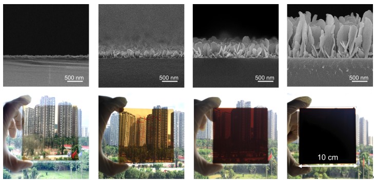
Figure 1. The tunable light trapping structure based on self-assembled SnSe2 nanoplate arrays (up to ~96%) (Image by CHEN Ming)
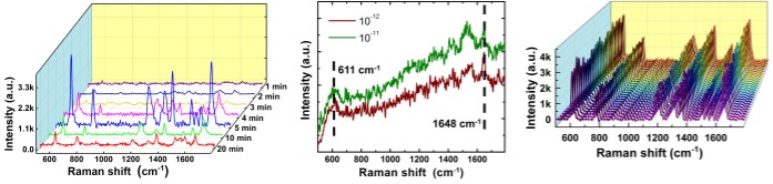
Figure 2. The SERS substrate based on self-assembled SnSe2 nanoplate arrays shows an ultralow detection limit (1×10-12 M), high enhancement factor (1.33 ×10⁶) and good uniformity (relative standard deviations down to 7.7%) (Image by CHEN Ming)
CONTACT:
ZHANG Xiaomin
Email: xm.zhang@siat.ac.cn
Tel: 86-755-86585299